| <<< Quadcopter JJRC H106 | Double H bridge from PCBWay v1.3 >>> |
H bridge Demo Board from PCBWay
The gadget in moving pictures with audio
The PCB shown in the video was provided to me by PCBWay. You can commission your own circuit board on their website:
https://www.pcbway.com/
By purchasing via the specified affiliate links, you support HOITG without any additional costs for you - thanks!
You can find the chapters (including videos) on what can be done with this demo board on my second project HomoFaciens.
How Open Is This Gadget?
The design data required to manufacture a circuit board can be created with open source software. I used KiCAD for this project.The design files of this freely programmable H Bridge ara available as Download-Package.
The PCB of the double H bridge in detail
Figure 1: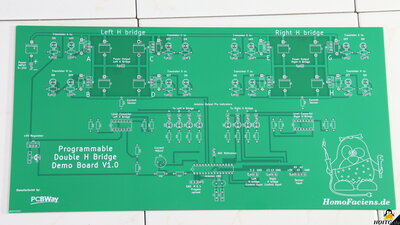
The professionally manufactured boards from PCBWay have a number of advantages:
First of all, the board is rock solid!
The copper wires of my handmade circuits bend easily and every now and then a soldered joint breaks. On the PCB, the conductive copper tracks are covered with an insulating layer of plastic film, which minimizes the risk of accidentaly shorting traces. All components are labeled and can therefore be referenced more easily.
The possibility of having any lettering or graphics printed on the surface makes the circuit board widely self-explanatory. The print is of high quality, even small letters are clearly readable and the fine lines of the graphic have smooth edges.
Technical data
| Category | Value | Remark |
|---|---|---|
| Dimensions |
330x160mm |
|
| Weight |
200g |
|
| Layers | 2-Layers |
Populating
Figure 2: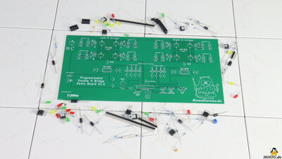
Thanks to the labels, populating the circuit board is quite easy and errors are minimized. The subsequent soldering on the back of the circuit board is also done very quick. This is mainly due to the applied soldering mask, which is a heat-resistant plastic coating that exposes the blank metal only on the soldering points. Thus, the solder is limited to the specified area, which means that even not so skilled tinkerers can produce error-free solder joints. The solder mask is particularly helpful when soldering points being close together, such as on the sockets for the ICs. Solder spatter or flux residue can be easily wiped off the plastic coating.
The result is a professional, easy-to-use circuit board - as said before, the explanation of how that double H bridge works can be found on my project HomoFaciens.
Design
Figure 3: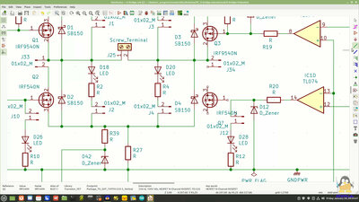
I created the board with the open source software KiCAD. The design process start with drawing the circuit. The next step is to create the layout. The components are first arranged on the virtual circuit board. The tracks are then drawn semi-automatically. Once the outer edges have been set, the required design data can be plotted, which means be exported.
There is an excellent documentation on using the software available on the KiCAD website.
These must now be uploaded to PCBWay.com via the online shop and a few other parameters, such as the board material and color must be specified. PCBWay accepts the data created by KiCAD after verification by an employee. It is only checked whether the board can be produced according to the files received, not whether you have produced any error in the circuit logic! After this step, it only takes a few days for the finished board to arrive - the production progress can be monitored on the PCBWay website.
The design files of this H Bridge ara available as Download-Package.
My conclusion
Going from an idea to a finished, professional circuit board is no rocket science! There's plenty of information on what can be controlled with a double H-bridge on my second project: HomoFaciens.| <<< Quadcopter JJRC H106 | Double H bridge from PCBWay v1.3 >>> |
![]()
![]()
![]()